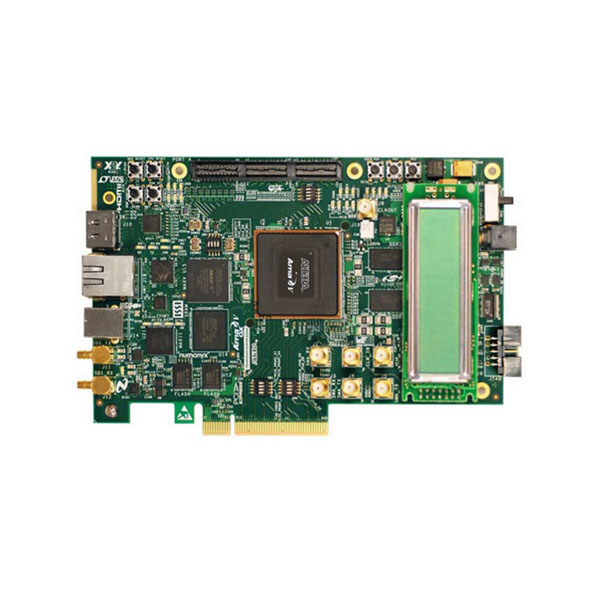
【DK-START-5AGXB3N】Altera Arria V GX Starter Kit
- 产品型号: DK-START-5AGXB3N/A5SK(Part No:T0111)
- 产品品牌: TERASIC友晶科技/Intel FPGA
- 产品规格: Arria V GX 5AGXFB3H4F35C5NES
- 产品价格: 7,650
- 咨询热线:027-87538900
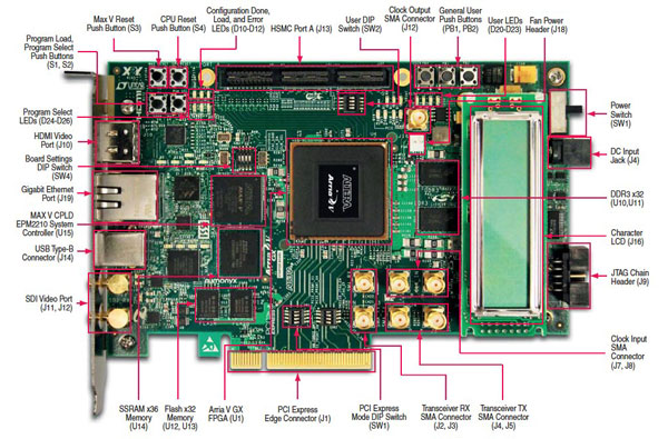
The Altera® Arria® V GX Starter Kit provides a complete design environment that includes all the hardware and software you need to develop cost-sensitive FPGA applications immediately. The development kit is RoHS compliant. The development kit features the following:
- Arria V GX FPGA—360KLE, F1152 package, 24X6.5G XCVRs, C4 speed grade
- One I/O expansion slot—one high-speed mezzanine card (HSMC) connector
- 256 MB of SDRAM memory
- High-definition multimedia interface (HDMI) and serial digital interface (SDI) connections
- SMAs
FPGA:
- Arria V GX 5AGXFB3H4F35C4N
System controller: MAX® V 5M2210ZF256C4N
- Power monitor GUI
- Single analog-to-digital converter (ADC), eight channels
- Non-isolated power rail
- Fast passive parallel (FPP) x16 mode through parallel flash loader (PFL)
- Control and status registers
Embedded USB-BlasterTM II:
- MAX II EPM570GM100C4N
HDMI 1.3 TX
- x4 XCVR, 2.7 Gbps (max by level shifter) and 270 MHz TX clock HDMI TX connector
- STMicroelectronics HDMI level shifter STHDLS101T
- Level shift XCVR PCML 1.5V <-> TMDS level
- DDC and HPD <-> HDMI compliant level
- Data channel up to 2.7 Gbps; HDMI 1.3 compliant
- Clock channel up to 270 MHz; enough to support 2.7 Gbps data rate
- HDMI specification: clock period = 10x of UI
SDI 3G
- x1 XCVR TX/RX loopback
- x2 SMB connectors and cable (cable not included in kit)
- Up to 2.97 Gbps
- Uses National Semiconductor driver/receiver LMH0384SQ/LMH0303SQx
- Requires 148.5 MHz and 148.35 MHz at XCVR refclk to support US and EU standard respectively
- Use VCXO to fine tune and lock to the recovered CDR frequency
HSMC
- x8 XCVR up to 6.375 Gbps
- Not complied to PCI Express® (PCIe® ) HIP pin assignment
- x4 CMOS
- x8 TX and x9 RX differential interface using dedicated TX/RX channels
- x2 low-voltage differential signalling (LVDS) clock in
- x2 differential clock out
- I2C
- JTAG
- Minimum current support
- 2A @ 3.3V
- 1A @ 12V
- Dedicated clock domain from Si 5338 clock generator for xcvr refclk
- HSMC loopback with BTS GUI
SMA
- 1x XCVR TX/RX channel
- 1x LVPECL clock input
- 1X LVPECL clock output
Clocking
- Dedicated clock domain from Si 5338 clock generator for xcvr refclk
DDR3 SDRAM x32
- Micron MT41J64M16LA-15E DDR3 SDRAM 8MX16X8
- Two devices: 2 x16 width = x32
- BTS DDR3 SDRAM GUI using Uniphy and high performance (HP) controller II
SSRAM
- 512k x36, 18 Mb ISSI IS61VPS51236A
- Shared address or data with flash
User IO
- LCD character
- x4 DIP switch
- x3 PB
- x4 LED
Configuration
- FPP x16 mode
- Dual flash 512Mbit Numonyx PC28F512P30BF (52 MHz FMAX )
- JTAG header
Embedded USB Blaster II
- Cypress Microcontroller CY7C68013A as USB PHY 2.0
- MAX II
Ethernet
- 10/100/1000 Base-T
- RJ-45 connector, on-board LED for link status
- Marvell Ethernet PHY 88E1111
- Requires 50 MHz clock from CLKIN
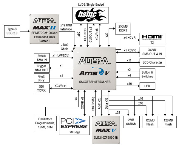
Altera Arria V GX Starter Board Block Diagram
| No | 产品名称 | 售价(RMB) |
|---|---|---|
| 1. |
[A5SK] Altera Arria V GX Starter Kit
产品编号: T0111
 重量: 3,500g 重量: 3,500g |
¥7,650 |


