产品展示
-
- Intel FPGA-Altera Stratix母板Intel FPGA-Altera Arria母板Intel FPGA-Altera Cyclone母板Intel FPGA-Altera MAX母板Intel FPGA-Altera 多媒体子板Intel FPGA-Altera 界面转换子板 Intel FPGA-Altera 影像显示类子板Intel FPGA-Altera 网路子板Intel FPGA-Altera 类比/数位转换子板Intel FPGA-Altera RF子板Intel FPGA-Altera USB BlasterIntel FPGA-Altera配件Intel FPGA-Altera机器人套件TI系列-C6000 DSP|ARMTI系列-C5000 DSPTI系列-C2000 DSPTI系列-DaVinci|SitaraIntel FPGA-Altera Agilex母板TI系列-仿真器FPGA|DSP|ARM|EDA|SOC教学实验箱
推荐产品

咨询热线:
18062095810
邮件: wangting@whhexin.com
电话:18062095810
地址: 湖北·武汉·鲁巷·华乐商务中心1006
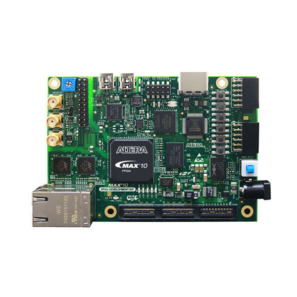
【M10K】TERASIC友晶 ALTERA MAX 10 FPGA DEVELOPMENT KIT
- 产品型号: M10K
- 产品品牌: TERASIC友晶科技/Intel FPGA
- 产品规格:
- 产品价格: 欢迎咨询采购,量多优惠多,提供完善的售后保障和支持!
- 咨询热线:18062095810
The Altera® MAX® 10 FPGA Development Kit provides a full featured design platform built around a 50 K logic elements (LEs) MAX 10 FPGA, optimized for system level integration with on-die analog-to-digital converter (ADC), dual-configuration flash, and DDR3 memory interface support. The board features on-board USB-BlasterTM II, high-speed mezannine card (HSMC), and Pmod™ Compatible expansion cards, high-definition multimedia interface (HDMI) output, and dual Ethernet for industrial Ethernet applications. The MAX 10 FPGA Development Kit provides the perfect system-level prototyping solution for industrial, automotive, consumer, and many other market applications.
With this development board, you can:
- Develop designs for the 10M50D, F484 package FPGA
- Measure the performance of the MAX 10 FPGA analog-to-digital block conversion
- Interface MAX 10 FPGAs to DDR3 memory at 300 MHz performance
- Run embedded Linux using the Nios® II processor
- Interface to daughtercards and peripherals using HSMC and Digilent Pmod™ Compatible connectors
- Measure FPGA power (VCC_CORE and VCC_IO ) using the power monitor graphical user interface (GUI)
- Reuse the kit’s PCB board and schematic as a model for your design
MAX 10 FPGA Development Board Block Diagram

The MAX 10 FPGA Development Kit includes the following:
-
RoHS- and CE-compliant MAX 10 FPGA development board
-
Featured devices
- MAX 10 FPGA (10M50D, dual supply, F484 package)
- Enpirion® EN2342QI 4A PowerSoC voltage-mode synchronous step-down converter with integrated inductor
- Enpirion EN6337QA 3A high-efficiency PowerSoC DC-DC step-down converters with integrated inductor
- Enpirion EP5358xUI 600 mA PowerSoC DC-DC step-down converters with integrated inductor
- MAX II CPLD – EPM1270M256C4N (On-board USB-Blaster II)
-
Programming and Configuration
- Embedded USB-Blaster II (JTAG)
- Optional JTAG direct via 10-pin header
-
Memory devices
- 64Mx16 1 Gb DDR3 SDRAM with soft memory controller
- 128Mx8 1 Gb DDR3 SDRAM with soft memory controller
- 512Mb quad serial peripheral interface (quad SPI) flash memory
-
Communication ports
- Two Gigabit Ethernet (GbE) RJ-45 ports
- One mini-USB2.0 UART
- One HDMI video output
- One universal HSMC connector (see HSMC expansion cards )
- Two 12-pin Digilent Pmod™ Compatible connectors (see Pmod™ Compatible expansion cards )
-
Analog
- Two MAX 10 FPGA ADC SMA inputs
- 2x10 ADC header
- Potentiometer input to ADC
- One external 16 bit digital-to-analog converter (DAC) device with SMA output
-
Clocking
- 25 MHz single-ended, external oscillator clock source
- Silicon labs clock generator with programmable frequency GUI
-
Switches, push buttons, jumpers, and status LEDs
-
-
Mini-USB cable for on-board USB-Blaster II
-
2A power supply and cord
-
Free Quartus® Prime Lite design software (download software and license from the website)
-
Complete documentation
- User manual, bill of materials, schematic, and board files
| No | 产品名称 | 售价(RMB) |
|---|---|---|
| 1. |
[M10K] ALTERA MAX 10 FPGA DEVELOPMENT KIT
产品编号: T0198
 重量: 1,400g 重量: 1,400g |
xxx |
Related Links
Documents
| 标题 | 版本 | 档案大小(KB) | 新增日期 | 下载 |
|---|---|---|---|---|
| User Guide |
1.0  |
2015-12-01 | ||
| Rev C Schematic |
1.0 |
2015-12-01 | ||
| Rev C. PCB Complete kit installation (Windows PC only) |
1.0 |
2015-12-01 | ||
| Rev B Schematic |
1.0 |
2015-12-01 | ||
| Rev B. PCB Complete kit document installation (Windows PC only) |
1.0 |
2015-12-01 |