产品展示
-
- Intel FPGA-Altera Agilex母板 Intel FPGA-Altera Stratix母板 Intel FPGA-Altera Arria母板 Intel FPGA-Altera Cyclone母板 Intel FPGA-Altera MAX母板 Intel FPGA-Altera 多媒体子板 Intel FPGA-Altera 界面转换子板 Intel FPGA-Altera 影像显示类子板 Intel FPGA-Altera 网路子板 Intel FPGA-Altera 类比/数位转换子板 Intel FPGA-Altera RF子板 Intel FPGA-Altera机器人套件 Intel FPGA-Altera USB Blaster Intel FPGA-Altera配件 FPGA|DSP|ARM|EDA|SOC教学实验箱 TI系列-C6000 DSP|ARM TI系列-C5000 DSP TI系列-C2000 DSP TI系列-DaVinci|Sitara TI系列-仿真器
推荐产品
- FPGA综合实验台 HC-STD-M
- 【DPO7254C】Tektonix泰克 高级信号分析示波器
- 【TMS320C6655/57】Tronlong创龙TL665xF-EasyEVM开发板
- HKMX-30型 十字路口交通信号灯实训装置
- 【SFP】TERASIC友晶SFP-HSM子板
- 【XAUI-SFP】DUAL XAUI TO SFP+ HSMC BOARD
- 【DK-DEV-1SGX-H-A】Intel Stratix 10 GX FPGA Development Kit
- 【TDS2024C】Tektonix泰克 200MHz示波器
- 【6221】Tektonix泰克 精密电流源
- 【DS1202Z-E】RIGOL普源 200MHz数字示波器

咨询热线:
18062095810
邮件: wangting@whhexin.com
电话:027-87538900
地址: 湖北·武汉·鲁巷·华乐商务中心1006
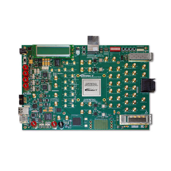
【DK-SI-5SGXEA7N/S5GSI】Altera Transceiver Signal Integrity开发板
- 产品型号: DK-SI-5SGXEA7N/S5GSI(Part No:T0118)
- 产品品牌: TERASIC友晶科技/Intel FPGA
- 产品规格: Stratix V GX FPGA:5SGXEA7N2F40C2N
- 产品价格: 欢迎咨询采购,量多优惠多,提供完善的售后保障和支持!
- 咨询热线:18062095810
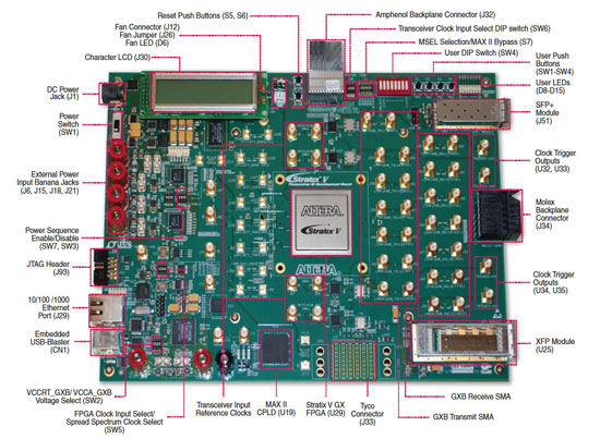
The Altera® Stratix® V GX Transceiver Signal Integrity (SI) Development Kit provides a platform for electrical compliance testing and interoperability analysis. The accessibility to multiple channels allows for real-world analysis as implemented in the system with transceiver channels available through SMA and popular backplane connectors. You can use this development kit to perform the following tasks:
Evaluate transceiver link performance from 600 Mbps to 12.5 Gbps
Generate and check pseudo-random binary sequence (PRBS) patterns via a simple to use GUI (does not require the Quartus® II software)
Access advanced equalization to fine tune link settings for optimal bit error ratio (BER)
Perform jitter analysis
Verify physical medium attachment (PMA) compliance to 10GbE, 10GBASE-KR, PCI Express® (PCIe®)(Gen1, Gen2, and Gen3), Serial RapidIO®, Gigabit Ethernet, 10-Gigabit Ethernet XAUI, Common Electrical I/O (CEI) 6G, CEI-11G, high-definition serial digital interface (HD-SDI), Interlaken, and other major standards
Use the built-in high speed backplane connectors to evaluate custom backplane performance and evaluate link BER
Featured device
Configuration status and set-up elements
Clocks
General user input/output
Memory devices
High speed serial interfaces
Power
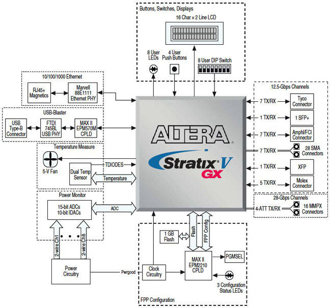
Stratix V GX Transceiver Signal Integrity Development Board Block Diagram
Laptop DC input
Voltage margining
Seven channels to Molex® Impact® connector
Seven channels to Amphenol® XCede®
Seven channels to footprint of Tyco Strada® Whisper® (connector is not populated)
Short trace routed on a micro-strip
Six strip-line channels from the with all the trace lengths are matched across channels
Seven full-duplex transceiver channels routed to SMA connectors
21 full-duplex transceiver channels routed to backplane connector
128-megabyte (MB) sync flash memory (primarily to store FPGA configurations)
10-/100-/1000-Mbps Ethernet PHY (RGMII) with RJ-45 (copper) connector
16x2 character LCD
One 8-postion dipswitch
Eight user LEDs
Four user pushbuttons
50 MHz, 125 MHz, programmable oscillators (preset values: 624 MHz, 644.5 MHz, 706.25 MHz, and 875 MHz)
SMA connectors for supplying an external differential clock to transceiver reference clock
SMA connectors for supplying an external differential clock to the FPGA fabric
SMA connectors to output a differential clock from the FPGA's phase-locked loop (PLL) output pin
JTAG
On-board USB-BlasterTM
Fast passive parallel (FPP) configuration via MAX® II device and flash memory
Two configuration file storage
Temperature measurement circuitry (die and ambient temperature)
5SGXEA7N2F40C2N
| No | 产品名称 | 售价(RMB) |
|---|---|---|
| 1. |
[S5GSI] Altera Transceiver Signal Integrity Development Kit, Stratix V GT Edition
产品编号: T0118  重量: 4,000g 重量: 4,000g | xxx |
Documents
CD-ROM
| 标题 | 版本 | 档案大小(KB) | 新增日期 | 下载 |
|---|---|---|---|---|
| Kit installation (for boards with ES silicon) | 11.1.2 | 2013-01-03 |  | |
| Kit installation | 12.0 | 2013-01-03 |  |


