产品展示
-
- Intel FPGA-Altera Agilex母板 Intel FPGA-Altera Stratix母板 Intel FPGA-Altera Arria母板 Intel FPGA-Altera Cyclone母板 Intel FPGA-Altera MAX母板 Intel FPGA-Altera 多媒体子板 Intel FPGA-Altera 界面转换子板 Intel FPGA-Altera 影像显示类子板 Intel FPGA-Altera 网路子板 Intel FPGA-Altera 类比/数位转换子板 Intel FPGA-Altera RF子板 Intel FPGA-Altera机器人套件 Intel FPGA-Altera USB Blaster Intel FPGA-Altera配件 FPGA|DSP|ARM|EDA|SOC教学实验箱 TI系列-C6000 DSP|ARM TI系列-C5000 DSP TI系列-C2000 DSP TI系列-DaVinci|Sitara TI系列-仿真器
推荐产品
- FPGA综合实验台 HC-STD-M
- 【DPO7254C】Tektonix泰克 高级信号分析示波器
- 【TMS320C6655/57】Tronlong创龙TL665xF-EasyEVM开发板
- HKMX-30型 十字路口交通信号灯实训装置
- 【SFP】TERASIC友晶SFP-HSM子板
- 【XAUI-SFP】DUAL XAUI TO SFP+ HSMC BOARD
- 【DK-DEV-1SGX-H-A】Intel Stratix 10 GX FPGA Development Kit
- 【TDS2024C】Tektonix泰克 200MHz示波器
- 【6221】Tektonix泰克 精密电流源
- 【DS1202Z-E】RIGOL普源 200MHz数字示波器

咨询热线:
18062095810
邮件: wangting@whhexin.com
电话:027-87538900
地址: 湖北·武汉·鲁巷·华乐商务中心1006
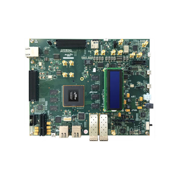
【DK-DEV-5ASTD5N】Arria V SoC Development Kit
- 产品型号: DK-DEV-5ASTD5N/A5SOC(Part No:T0454)
- 产品品牌: TERASIC友晶科技/Intel FPGA
- 产品规格: Arria V ST SoC—5ASTFD5K3F40I3N (SoC)
- 产品价格: 欢迎咨询采购,量多优惠多,提供完善的售后保障和支持!
- 咨询热线:18062095810
The Altera® Arria® V SoC Development Kit offers a quick and simple approach to develop custom ARM® processor-based SoC designs. Altera’s midrange, transceiver-based Arria V FPGA fabric provides the highest bandwidth with the lowest total power for midrange applications such as:
Remote radio units*
10G/40G line cards*
Medical imaging
Broadcast studio equipment.
Acceleration of image- and video-processing applications*
PCI Express® (PCIe®) Gen2 x4 lanes (endpoint or rootport)
Featured devices
Arria V ST SoC—5ASTFD5K3F40I3NES (SoC)
MAX® V CPLD—5M2210ZF256C4N (system controller)
MAX II CPLD—EPM570GF100 (embedded USB-BlasterTM II cable)
FPGA configuration sources
Embedded USB-Blaster II (JTAG) cable
EPCQ flash (Active Serial x1 or x4 configuration)
Flash fast passive parallel (FPP)
Hard processor system (HPS)
FPGA memory
2x 1,024 MB 32-bit DDR3 SDRAM
1x 512 Megabit (Mb) CFI synchronous Flash
1x 256 Mb NOR Flash (EPCQ)
FPGA I/O interfaces
1x PCI Express x4 Gen2 socket
2x FPGA mezzanine card (FMC) portds
2x 10/100 Ethernet ports
2x SPF+ ports
4x user LEDs
4x user pushbuttons
4x user dip switches
HPS boot sources
512 Mb QSPI Flash
Removable micro-SDCard flash
FPGA
HPS memory
1x 1,024 Mbyte (MB) DDR3 SDRAM with ECC
1x 512 Mb QSPI flash
Micro-SDCard socket with 4 GB micro-SDCard flash device
One 32 Kb I2C serial EEROM
HPS I/O interfaces
1x 1 Gigabit Etherent port (HPS)
1x USB 2.0 on-the-go (OTG) port (HPS)
2x RS-232 UART (through mini-USB port)
x1 real-time clock (with battery backup)
x1 two-line text LCD
x4 user LEDs
x4 user push buttons
x4 DIP switches
Clocking
Four-output programmable clock generator for FPGA reference clock inputs
148.5 MHz LVDS programmable voltage-controlled crystal oscillator (VCXO) for FPGA reference clock input
50 MHz single-ended oscillator for FPGA and MAX V FPGA clock input
100 MHz single-ended oscillator for MAX V FPGA configuration clock input
SMA inputs for FPGA and HPS clocks
LMK04828 clock jitter cleaner
Power
Laptop DC input 14—20 V adapter
System monitoring circuit
Power (voltage, current, wattage)
Mechanical
Board dimensions—7.175” x 9”
SoC Embedded Design Suite Subscription Edition
ARM Development Studio 5 (DS-5™) Altera Edition Toolkit
Hardware-to-software handoff tools
Linux run-time software for application development
SoC hardware libraries for firmware development
Application examples
| No | 产品名称 | 售价(RMB) |
|---|---|---|
| 1. |
[A5SOC] Altera Arria V SoC Development Kit and SoC Embedded Design Suite
产品编号: T0235  重量: 3,400g 重量: 3,400g | xxx |
Documents
| 标题 | 版本 | 档案大小(KB) | 新增日期 | 下载 |
|---|---|---|---|---|
| Arria V SoC Development Kit User Guide | 1.0 | 3136 | 2014-06-04 |  |
| Arria V SoC Development Board Reference Manual | 1.0 | 1978 | 2014-06-04 | |
CD-ROM
| 标题 | 版本 | 档案大小(KB) | 新增日期 | 下载 |
|---|---|---|---|---|
| Kit installation (EXE) (Windows) | 13.1.0.5 | 2014-06-04 |  | |
| Kit installation (ZIP) (Linux) | 13.1.0.5 | 2014-06-04 | |